The market for probe card manufacturing is expected to witness a significant growth in the coming years. This is mainly due to the increase in demand for smart wearables and smartphones. Probe cards are a type of test card used to check the quality of ICs produced by semiconductor manufacturers. Typically, these testers are used for testing DRAM and FLASH memory devices.
Cost
The cost of probe card manufacturing is dependent on the types of contact elements used in a probe. This includes the material, thickness, and shape of the contact. It can also be affected by the type of wafer a device is being tested on.
As the semiconductor industry continues to grow and evolve, demand for more testing equipment is predicted to increase. This demand is driven by the shrinking size of ICs, the speed at which they must be tested, and their increased functionality.
The efficiency of the test process is impacted by the number of DUTs (Device-Units-To-Unit) that can be tested in parallel. In addition, the accuracy of the inspection process is also important to a product’s success. Worn or abnormal probe pins can cause incorrect inspection data to be acquired, which can lead to a decrease in yield rates.
Design
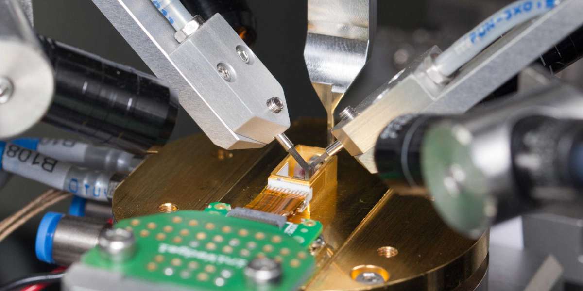
A probe card is a device that forms an electrical path between a semiconductor wafer and an external test system. It enables electrical testing of semiconductor chips before they are diced and packaged.
Designed to meet specific applications, probe cards are custom configured for testing wafers on manual and automatic probe stations. They can have complex layouts consisting of numerous DC contacts and multiple microwave probes with operating frequencies from 40 to 110 GHz.
The probe card manufacturing market is primarily driven by the increased integration of advanced technologies such as human-machine interface (HMI) in electronic devices. Additionally, the construction of new fabs to manufacture ICs is contributing to the market growth. This is due to the increasing demand for ICs in a variety of industries.
Flexibility
Probe cards are used to test the electrical characteristics of a semiconductor device during the manufacturing process. They are an essential part of the industry, and their demand is increasing due to increased chip complexity.
As a result, manufacturers are constantly reevaluating their design and adjusting their processes to test today’s devices in parallel. One of the main challenges in this regard is contamination build-up on probe tips due to successive touch down events, which can negatively affect contact resistance measurement and testing results.
AST offers solutions that help address these issues in the Probe Card manufacturing environment. These solutions are based on our extensive imaging expertise and automated positioning technology that delivers state-of-the art inspection metrology performance.
Performance
The performance of a probe card depends on a number of factors, including the amount of power delivered to an IC wafer. The probe tips have to be able to make contact with the metal pads on the IC wafer, so test signals can be passed from the tester to the IC.
Sensitive devices — such as flip chip die and those using low-k dielectrics — require special attention to avoid damage during testing. This requires reducing contact forces while maintaining sufficient contact resistance for all dies on the wafer.
As a result, probe card manufacturing have been making advances in their products to reduce contact forces and increase flexibility. These innovations include improved planarity, lithographically defined springs, and new probe tip materials.